Taiwan Tech’s World-First Rhombic Metallic Nanotube Array Boosts Biomedical Testing, Featured on Top Journal Cover.
A research team led by Professor Jinn Chu from the Department of Materials Science and Engineering at Taiwan Tech has recently developed the world’s first diamond-shaped metallic nanotube array. This innovative structure significantly enhances Raman scattering signals, accelerating molecular detection speed and improving sensitivity. The technology shows promising potential for applications in biomedical diagnostics, food safety, and environmental monitoring. The research was published in the Royal Society of Chemistry's flagship journal Nanoscale and was featured as the cover article, highlighting its innovative value in nanomaterial design and application.
Professor Chu explained that the team has been working on the development and optimization of metallic nanotube arrays since 2018. Through years of simulation and experimentation with various geometric structures - including circular, square, and equilateral triangle arrays—they ultimately identified the diamond-shaped structure as the most effective design for enhancing electromagnetic field hotspots. These “hotspots”, located at the sharp corners of the diamond shapes, are regions where electromagnetic fields are most concentrated. They dramatically amplify Raman scattering signals, enabling the rapid and precise identification of trace molecules. This advancement paves the way for high-speed, highly sensitive detection of toxins, drugs, or disease biomarkers.

Taiwan Tech recently developed the world’s first diamond-shaped metallic nanotube array, which enhances Raman scattering signals and improves the speed and sensitivity of molecular detection - enabling the identification of trace amounts of cancer cells or pesticide residues in samples. From left: research team member Chun-Ting Wang and Professor Jinn Chu from the Department of Materials Science and Engineering.
The diamond-shaped metallic nanotube array technology, which significantly enhances surface-enhanced Raman scattering (SERS) signals, has been published in the Royal Society of Chemistry’s flagship journal Nanoscale and selected as the cover article, highlighting its innovative value in nanomaterial design and application technologies.
This technology employs silver (Ag) as the material for the nanotubes. Research shows that, compared to gold or other metals, silver possesses superior surface plasmon resonance properties, which significantly enhance signal amplification. The nanotubes are deposited onto a silicon wafer substrate, with over 100 million diamond-shaped nanotubesaccommodated per square centimeter. By increasing the surface area, the structure boosts molecular adsorption and sensing capabilities, achieving a detection limit as low as 10⁻¹² molar concentration-far more sensitive than many traditional testing methods.
In the future, if integrated into rapid test kits, wearable health monitoring devices, or even extended to telemedicine equipment and daily monitoring tools in long-term care facilities or home healthcare, this innovation could address common issues found in conventional diagnostics - such as low sensitivity, complex sample processing, costly and difficult chip fabrication, and delays in obtaining results. It could greatly accelerate early disease detection for both doctors and the general public. For example, bodily fluids like blood or urine could be used for rapid screening of cancer, diabetes, and more. Additionally, when paired with microfluidic devices, it could be applied to food safety testing for detecting pesticide residues, ractopamine, and other contaminants.
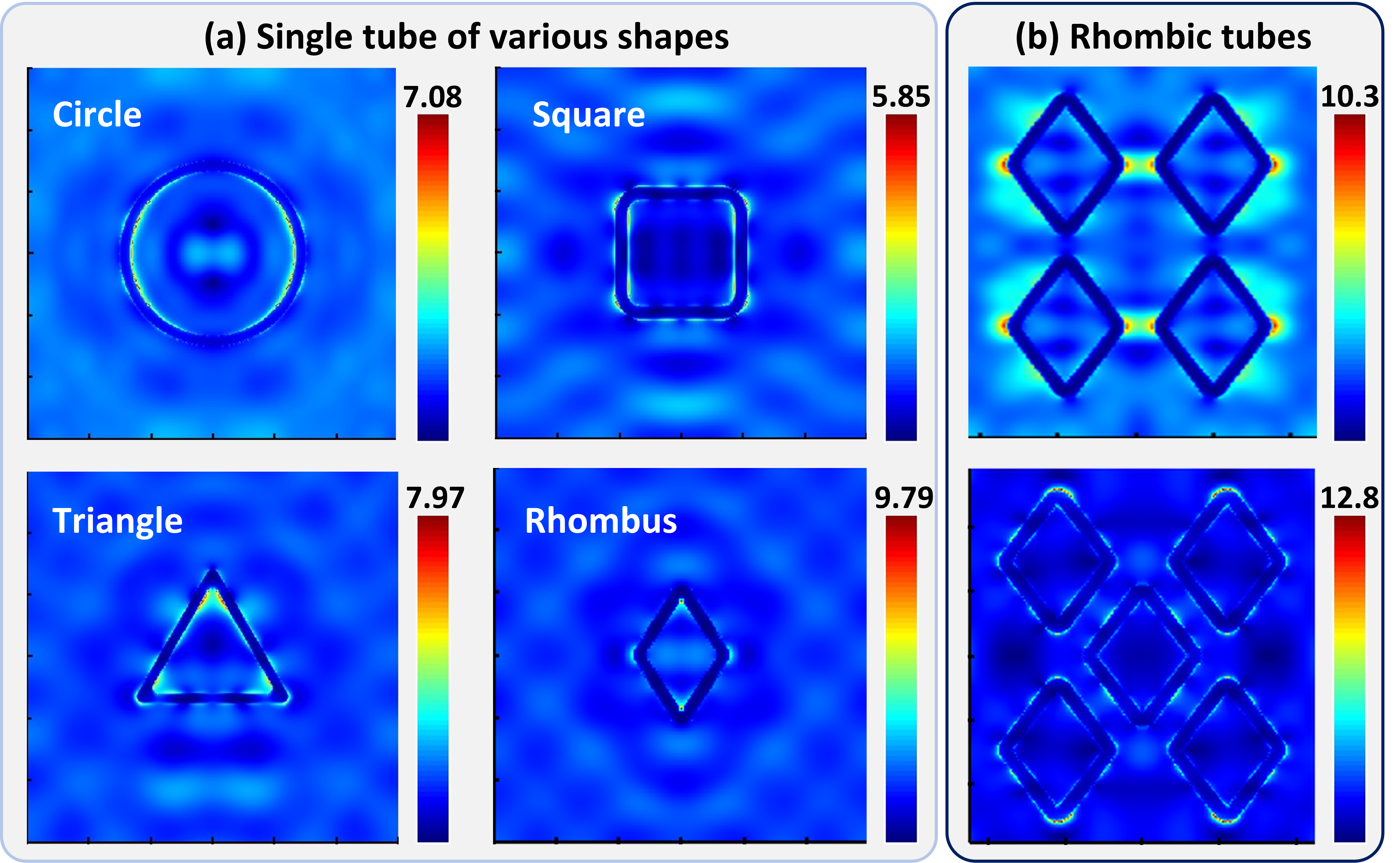
The research team evaluated the electromagnetic properties of four types of silver nanotubes - circular, square, and triangular - each with a height of 800 nm, and ultimately identified the diamond-shaped structure as the most effective geometric design for enhancing electromagnetic field hotspots. The electric field intensity of a single diamond-shaped nanotube reached 9.79, and when densely arranged, the field distribution increased further to over 12.
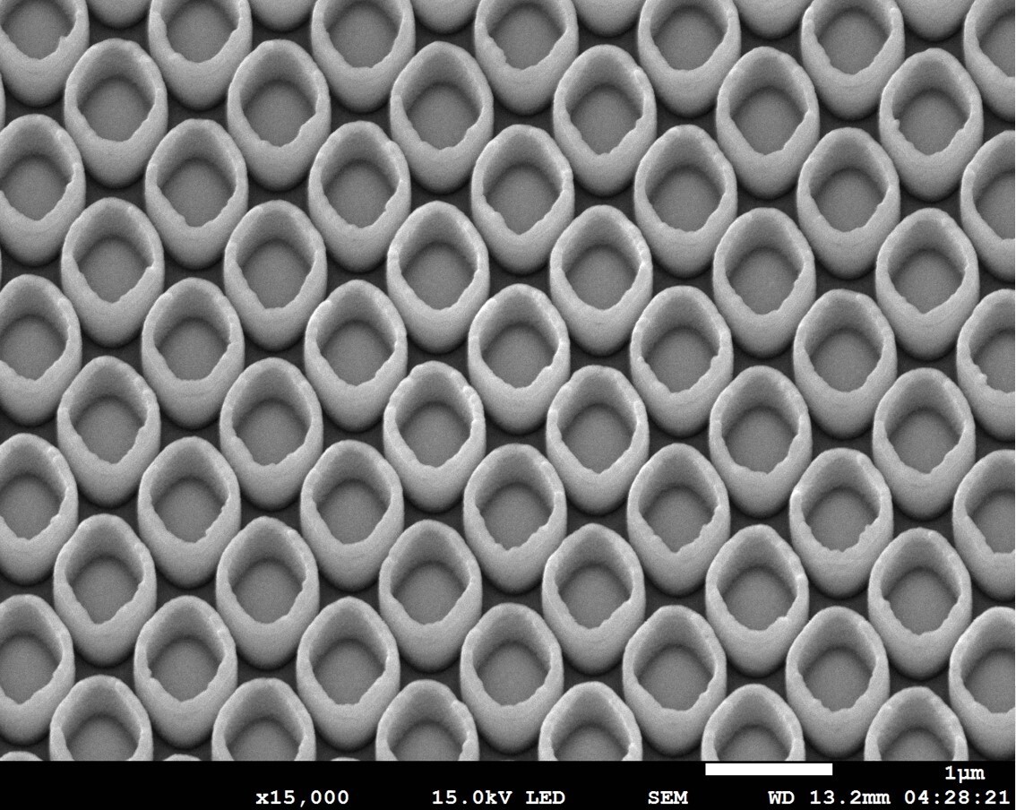
Using a scanning electron microscope at 15,000× magnification, the team observed that over 100 million diamond-shaped nanotubes can be accommodated per square centimeter of silicon wafer. The increased surface area enhances molecular adsorption and sensing capability, achieving a detection limit as low as 10⁻¹² molar concentration, which is significantly more sensitive than many conventional testing methods.
In addition to its sensing capabilities, the research team also discovered that the diamond-shaped metallic nanotube array exhibits excellent hydrophobicity and anti-frost properties. It can effectively delay the freezing of water droplets and reduce ice adhesion, making it a promising material for applications in aerospace components, outdoor sensors, and anti-frost coatings. These features expand the technology’s potential value in fields such as energy, environmental control, and smart devices.
The research team includes alumni Ting-Hao Chang, Alfreda Krisna Altama, and current second-year master’s student Chun-Ting Wang from the Department of Materials Science and Engineering. According to Wang, the technology was fabricated using standard processes commonly used in the semiconductor and MEMS industries, such as lithography, room-temperature sputtering, and lift-off techniques. Only minor adjustments are needed for integration into existing wafer foundry production lines, offering advantages such as low cost, large-area scalability, high reproducibility, and high yield. Compared to costly methods like electron beam lithography and FIB drilling, this approach is significantly more cost-effective.
Wang stated, “We believe this technology can dramatically improve the efficiency and convenience of medical diagnostics - from hospitals to homes, from clinical settings to individual users.” It holds promise for promoting an affordable, accessible, and highly accurate healthcare environment of the future, aligning with the core goals of preventive medicine and health promotion.
Professor Jinn Chu noted that the team is currently collaborating with major medical centers to conduct preliminary human trials on clinical samples, aiming to verify the feasibility and sensitivity of this technology for early cancer screening. At the same time, the team is in discussions with several domestic companies specializing in optical sensing applications, presenting the technology for performance validation and technical demonstrations. These efforts aim to explore opportunities for technology transfer and co-development, with the long-term goal of applying this innovation to precision health, smart sensing, and advanced semiconductor materials. Through these developments, the team hopes to accelerate the practical deployment of the technology and drive Taiwan’s sensor and smart healthcare industries toward their next stage of advancement.

The lithography, room-temperature sputtering, and lift-off techniques used by the research team are standard processes widely adopted in today’s semiconductor and MEMS industries. With only minor adjustments, the technology can be seamlessly integrated into existing wafer foundry production lines, offering advantages such as low cost, large-area scalability, high reproducibility, and high yield. The image shows the research team immersing the sample in 50 °C acetone for the lift-off process, completing the fabrication of the diamond-shaped silver nanotube chip.
The team is also actively working to extend the application of this technology to non-silicon substrates. Professor Jinn Chu explained, “We don’t just aim to fabricate nanotubes on silicon wafers - we hope to adapt the technology to other materials, such as steel, depending on industry needs.” In traditional industries, the high surface area provided by the nanotube structures can enhance reaction rates, catalytic performance, and adsorption capabilities, paving the way for innovative applications in smart manufacturing and materials engineering.
This research was selected as the cover article in Nanoscale, marking not only a milestone in the team’s years of technological development, but also a recognition of Taiwan’s strength in nanomaterials and smart sensing on the global stage. The team now feels even more confident in further extending and integrating the technology across various practical domains, advancing toward broader implementation and international collaboration.