Taiwan Tech launches Graduate Institute of Advanced Semiconductor Technology to advance silicon photonics and packaging.
To meet the rapidly evolving semiconductor industry and talent demands, Taiwan Tech has established the “Graduate Institute of Advanced Semiconductor Technology” in the 2024 academic year. The institute focuses on cutting-edge fields such as silicon photonics, compound semiconductor materials, and advanced packaging. Taiwan Tech is also riding the wave of AI, collaborating with industry partners to promote the development of advanced technologies. With the silicon photonics measurement and packaging equipment funded by the National Science Council’s “Crystal Innovation Program” the Hwahsia campus has been revitalized, offering a comprehensive learning and hands-on environment for both the industry and students. This initiative aims to expand industry-academia collaboration and enhance the effectiveness of semiconductor talent cultivation.
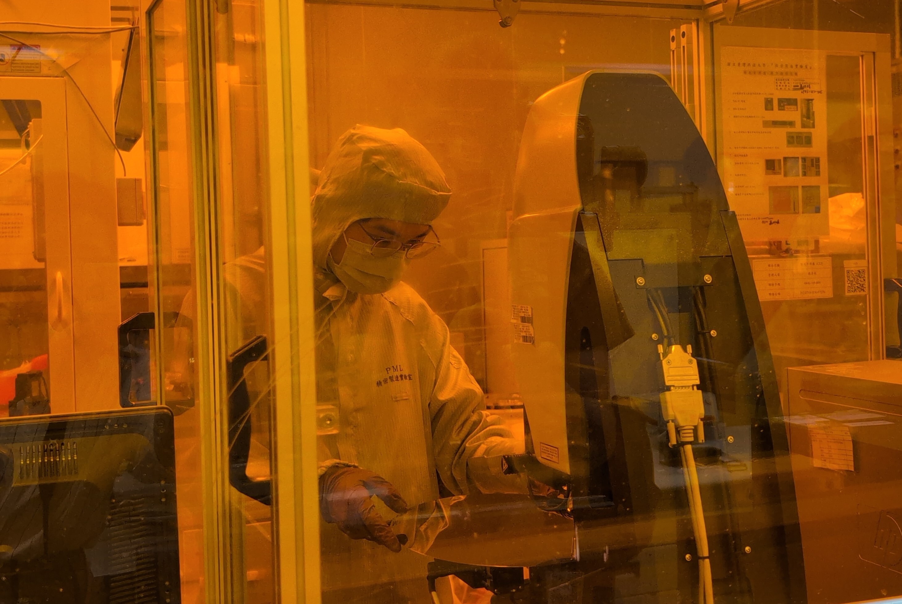
Taiwan Tech students use semiconductor surface inspection equipment for wafer quality testing.
In recent years, AI and semiconductor-related fields have become highly sought after, with many leading companies viewing “silicon photonics” as the next-generation technology to enhance data transmission speeds. Taiwan Tech President Jia-Yush Yen emphasized that while the industry advances, a continuous influx of talent is essential, stating, “Taiwan Tech must carve out its own space!” In addition to IC design, Taiwan Tech has many faculty members skilled in bridging theory with practice in backend packaging and testing. By leveraging cutting-edge equipment in silicon photonics and heterogeneous materials, along with internship opportunities at domestic and international companies and full scholarships, Taiwan Tech aims to cultivate highly skilled, industry-ready professionals.
Director of the Graduate Institute of Advanced Semiconductor Technology, Shih-Hsiang Hsu, highlighted that Taiwan Tech’s semiconductor research focuses on “silicon photonics”, “compound semiconductor materials”, and “advanced packaging technologies.” Silicon photonics, an innovative field combining optics and electronics, can enhance transmission speeds and reduce energy consumption during computing processes. This technology has applications in communication (6G), data transmission, advancing AI, machine learning, and high-performance computing. It is expected to significantly impact the future of the semiconductor industry, which is why many tech giants are investing heavily in R&D to capture the market for ultra-high-speed transmission chips.
The grating on the silicon chip can couple external light into the silicon photonic device, enhancing signal transmission efficiency while reducing energy consumption.
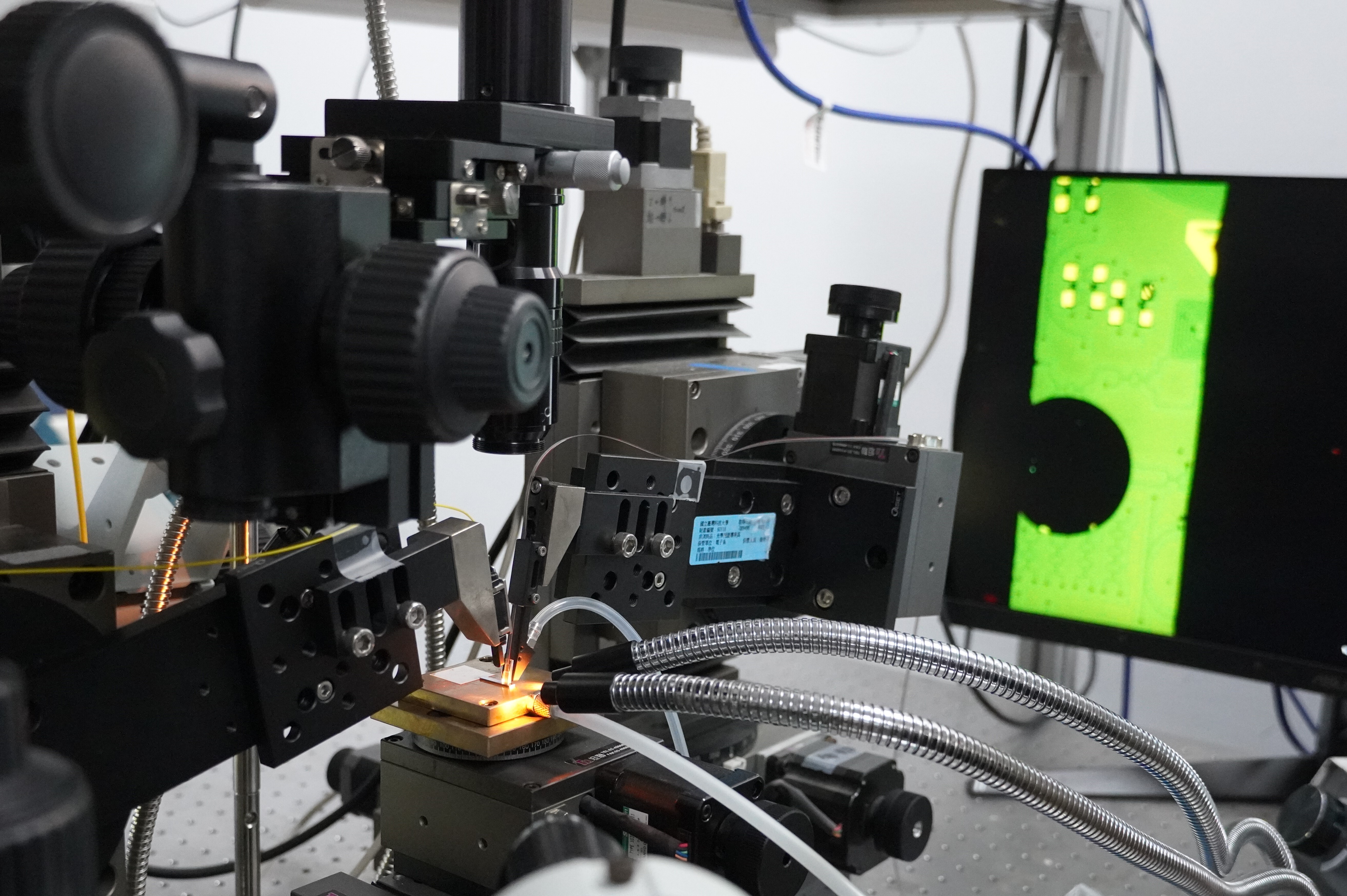
Taiwan Tech students operate a fiber-optic optical coherence tomography (OCT) system to inspect defects on chips, such as dents, micro-cracks, and voids.
The “Graduate Institute of Advanced Semiconductor Technology” plans to admit 36 master’s students and 5 doctoral students annually, enhancing the depth and breadth of talent development. Faculty will also invite industry experts to the classroom to guide students on the latest technologies and applications in the field, bridging the gap between academia and industry. Starting in 2025, the institute will begin enrolling international students, deepening global cooperation, and offering diverse learning and development opportunities to cultivate semiconductor professionals with an international perspective.
In addition to talent development, Taiwan Tech will establish the “Semiconductor Innovation and Application Research Center” at the Hwahsia campus, incorporating the silicon photonics automation measurement and packaging equipment purchased through the National Science Council’s Crystal Innovation Program. This will expand research and practical spaces for both faculty and students, revitalizing the Hwahsia campus.
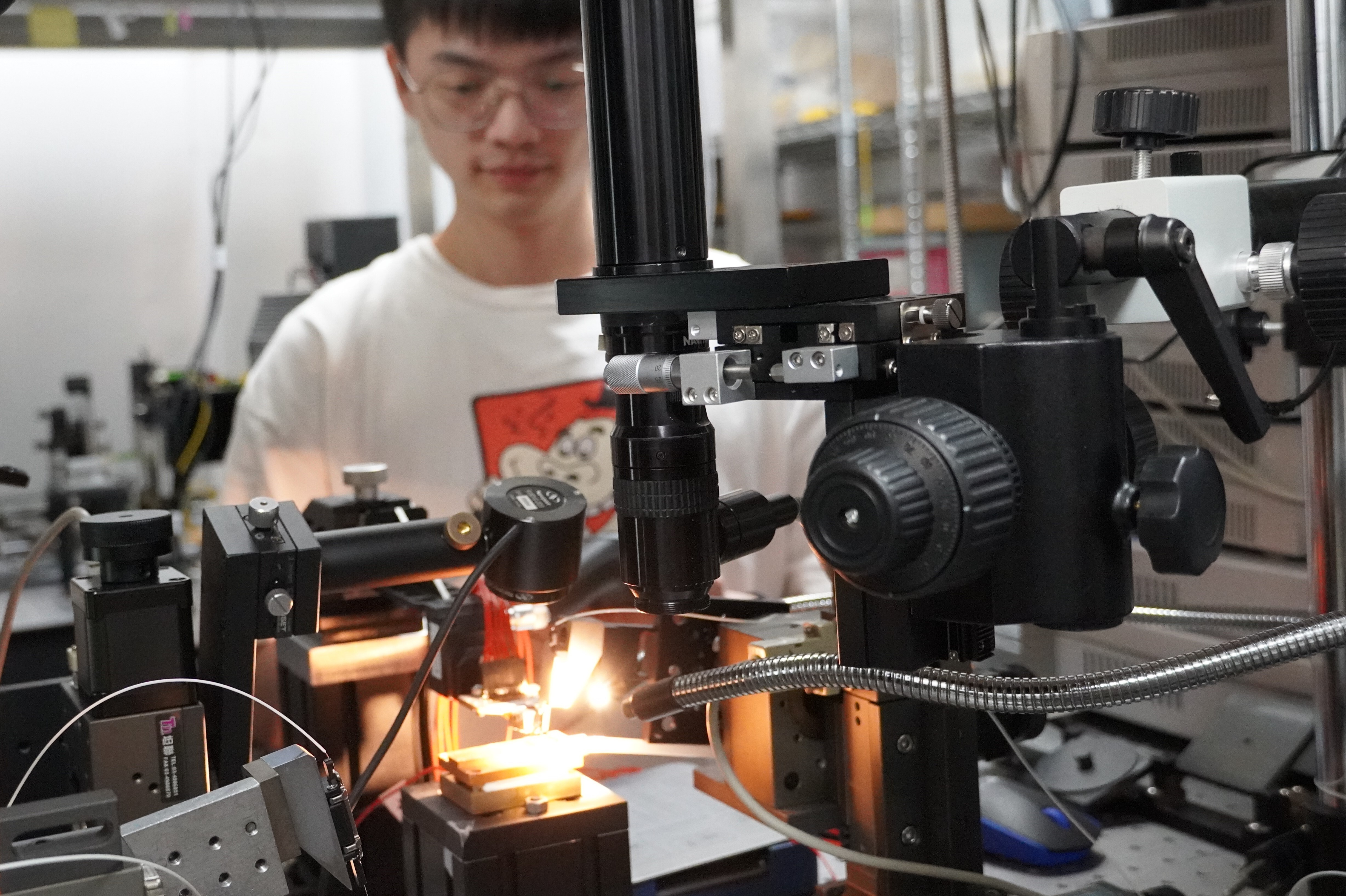
Taiwan Tech students demonstrate the beam steering function in a LiDAR system using a silicon photonics chip, which can be applied in the future to improve the computational efficiency of robot or vehicle navigation and obstacle avoidance.
With a diverse range of equipment, Taiwan Tech provides not only teaching, research, and hands-on production opportunities, but also a platform for industry collaboration and R&D. This allows faculty to teach semiconductor design, smart manufacturing, and packaging applications using real-world equipment. Additionally, the focus on silicon photonics equipment can be accessed through the Taiwan Semiconductor Research Institute (TSRI) equipment-sharing platform, enabling teams from academia, industry, and research institutions across Taiwan to reserve and utilize these advanced tools, thereby enhancing Taiwan’s competitiveness in the semiconductor industry.
By establishing the “Graduate Institute of Advanced Semiconductor Technology” and participating in the Crystal Innovation Program to set up key semiconductor equipment, Taiwan Tech is making a comprehensive effort to advance in the semiconductor field. The university is not only focused on developing cutting-edge technologies but also on cultivating more professionals with both practical experience and innovative capabilities. In the future, Taiwan Tech plans to integrate its extensive research resources, bridge the R&D needs of industries, and become a key player in strengthening Taiwan’s leading position in semiconductor manufacturing.
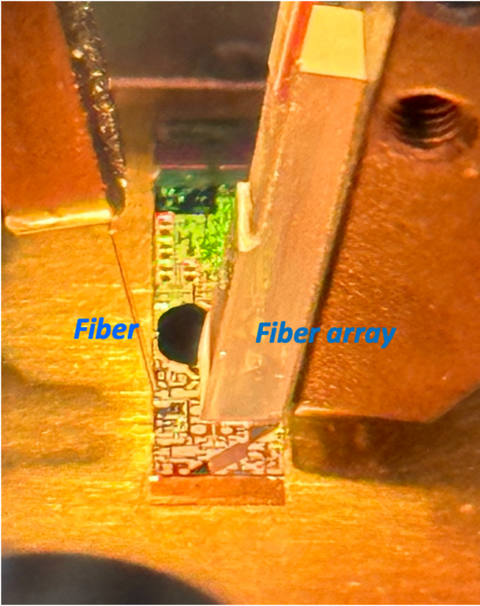
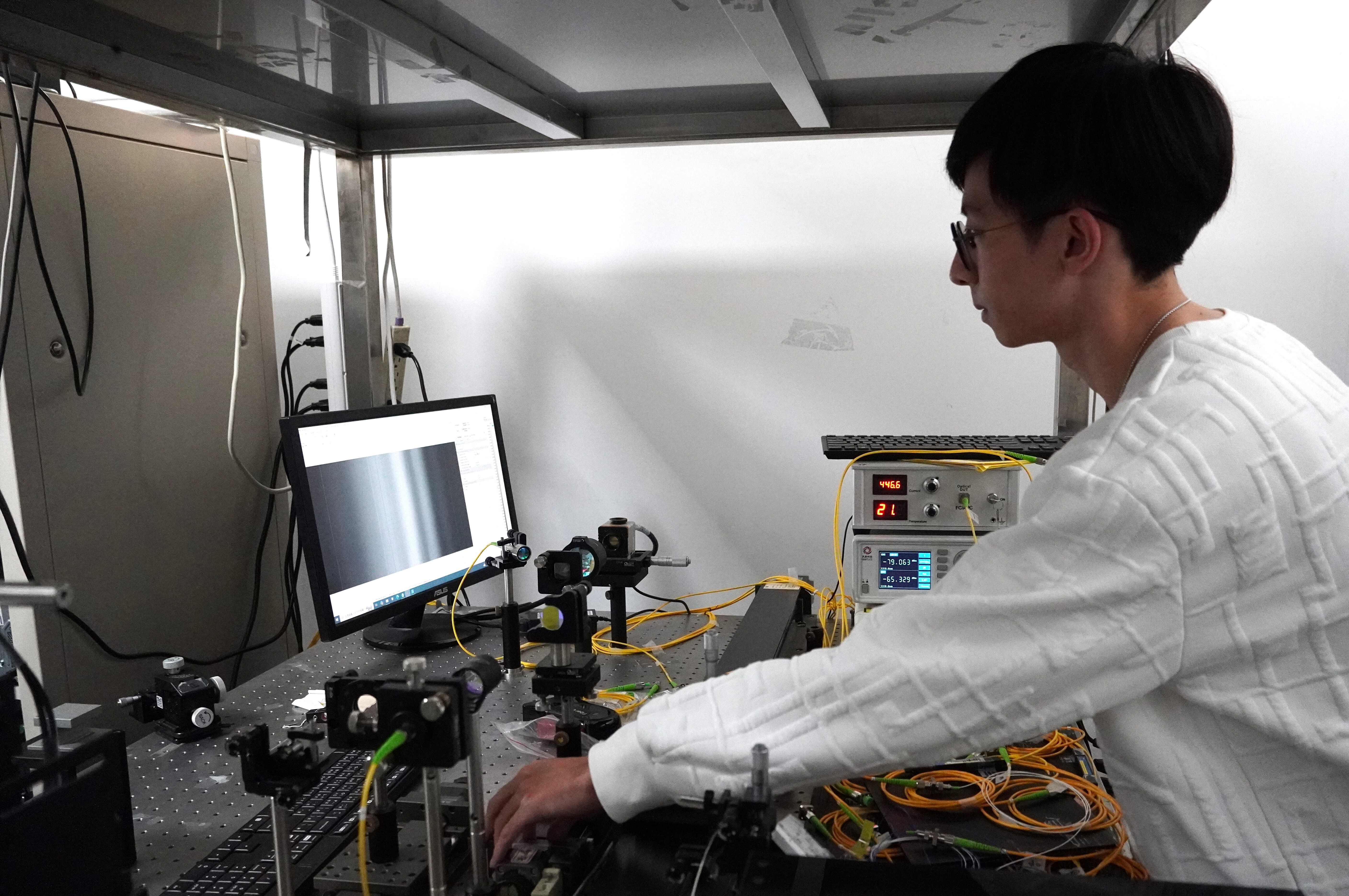
In the measurement system, the optical fiber is responsible for light input. Once the light signal enters, it is directed to the silicon photonics optical coherence tomography (OCT) chip, and then transmitted to the optical fiber array for image analysis.